The obvious disclaimer: the hack described in this article is not supported by the manufacturer, and may void your warranty. If you void your warranty, or just totally blow your motherboard by over-voltage or improper wiring in general, I don't accept any responsibility. You're on your own. The information is provided "as is". It may be incomplete and likely fits only a narrow subset of the hardware out there (my hardware setup is precisely specified below). The article is a result of my own detective work in chip datasheets and publically available information from third parties. None of it originates from MSI.
A friend of mine bought an MSI P7N SLI Platinum mainboard. Installed it in his PC chassis, put all the components in, installed Windows, and in good faith, installed the MSI auto-update utility. As this windows-based auto-update util kicked in, the first thing it offered was a BIOS update. And after the next reboot, the machine didn't boot. It didn't even give the usual beep code if the DIMMs were removed. Clearly the BIOS flash went awry.
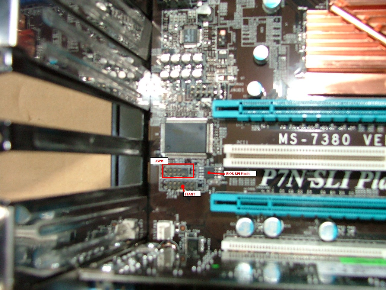
Based on some past reading of someone else's notes about the blessed SPI technology, I already knew what to look for when there was no obvious PLCC32 Flash on the motherboard, neither in a socket, nor soldered onboard. I found the culprit SPI Flash chip, in my case it was an MX25L8005 by Macronix International (MXIC) (datasheet available on the manufacturer's site, link too long/dynamic). But voila, in my case I could find a neat pin header nearby, labeled JSPI1 - clearly an SPI port for "manufacturer access". The 2mm spacing is a little hard to tap (difficult to get your hands on a female connector), but better than soldering the 8pin chip or sending the board for an RMA to TW and back.
This is where the JSPI1 connector is located:
Still I was a little reluctant to start some hacking around that. Out of the three local MSI importers/distributors, I managed to get someone on the phone at just one of them. He confirmed that there's no authorized local servicing center for MSI and that any flawed MSI hardware within warranty had to be shipped back to Taiwan. Which means a prospect of having your board repaired in maybe 2 months. Rather apalling. So I took the dive, downloaded the Flash chip's datasheet, started my multimeter and got on with the probing job.
Here's the pinout of JSPI1:
           ___
     Vcc  |o o|  Vcc
10   SO   |o o|   SI   9
 7   CS#  |o o| SCLK   8
     GND  |o o|  GND  18
     n.c. |o  |
          `---'
The two sideways columns of numbers are pin references to a standard PC parallel port (Canon DSUB25 male on the cable). Yes, it is possible to build a fairly simple passive adapter cable, even without a breadboard. See the aforementioned SPI flashing webpage by Rayer for a cable schematic. You only need to add a source of +3.3V for Vcc (see below). You'll also need an SPI flashing proggie coded by my friend Rayer. For DOS, which is my favourite OS for flashing, you also need a DPMI server, e.g. CWSDPMI. Just run CWSDPMI.EXE before SPIPGM.EXE.
MSI did their homework fairly well, to the extent that you can program the 8pin SMT chip in-circuit, provided that you provide a good enough external source of 3.3V. It seems that the board, if fully alive, pulls CS# low and provides clock to the SPI flash chip, which would hamper your in-circuit flashing attemtps. But, if the board is powered off, it doesn't interfere with the flash chip's pins (the relevant outputs of the south bridge / SuperIO companion are in hi-Z state. I haven't tried flashing the board on stand-by power - it might work even without an auxiliary source of +3.3V.
Anyway it's probably good practice to provide your own source of 3.3V. If you have a stabilized PSU with this sort of output, it's only appropriate to use it. I myself have solved the problem by tapping a classic internal HDD power connector (the red line) and connected two silicon diodes (not Schottky!) in series. The model I used was a small-signal 1N4148, which turned out to be fairly feeble. A 1A model like 1N4007 would be more appropriate. Some diodes may require you to insert 3 diodes in series. You have to test+measure this with some dummy load. The point is that each diode should provide a forward voltage drop of about 0.6-0.9 V. Schottky diodes give only about 0.3V of forward voltage drop. If you connect several of them in series, this turns your 5V line into something around 3.3V. My MX chip is guaranteed to work within 2.7-3.6 V, with the absolute maximum being 4.6V, so it can probably tolerate the hack with diodes, though the diode's tend to bend a lot under load. I've noticed this in my setup. With a 560Ohm dummy load, the two diodes gave about 3.6 V left. When I attached the motherboard, the output voltage of my hacked power source was down to 3V. It seems that the motherboard has quite some consumtion, e.g. the stand-by LED is alight! :-) It's certainly not just the SPI flash that gets powered. The 1N4148 actually get quite hot on the power dissipation (voltage drop times forward current).
Consider rounding this off by a relatively beefy electrolytic cap tapped straight on your cable, as close to the connector as possible. Mine was 1200 uF @ 6.3V. This should filter the Vcc line enough for stable SPI communications and flashing.
Maybe it would actually be much easier to just tap the 3.3V line straight from your desktop PC's ATX PSU connector. Stick an unfolded office clip into the cavity around an orange wire in the 20/24pin ATX plug. Still I guess additional filtering at the cable end would be appropriate.
And this is what my cable looks like in the end:
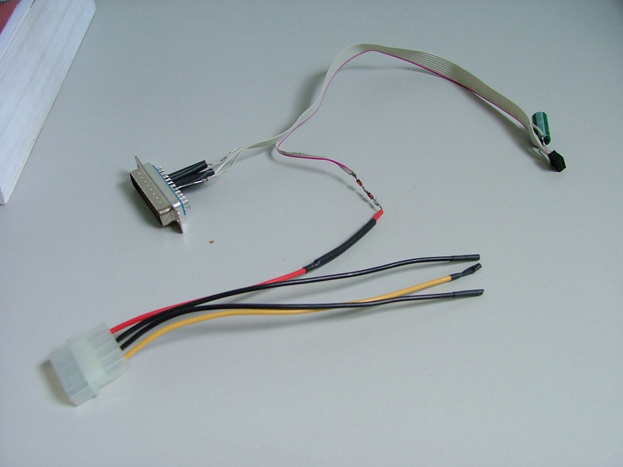
I deliberately don't publish a full schematic - work it out yourselfs. Let this be a proof that you're up to the hack, on the soldering side of things.
Things that might go wrong / might make you wonder:
SPIPGM.EXE can detect and report a few SPI chip models known to Rayer. But even if your Flash chip is not recognized as one of the well-known models, there's a good chance that SPIPGM will actually work. It certainly doesn't object, it merely asks about the size of the flash in kB. In my case, the MX25L8005 is an 8Mb chip, which means 1 MB, which equals 1024 kB. So I entered just 1024.
It's good practice to first make a backup of the original ROM contents (SPIPGM /d <filename>), then erase the Flash chip, then flash your desired image, then read back the contents and verify that the data got written correctly (compare the two binaries - I did this using md5sum, but some file managers can do it too). If the desired image and the dump that you read back don't match, look for the source of interference.
One possible source of interference can be the PSU. Mine was a problem, until I added the 1200uF filtering cap. I noticed the problem by touching the diodes while some SPI communications were going on - the StandBy LED went dark :-) Not anymore, once I added that filter cap.
Another problem could stem from a slow LPT port. Rayer addresses this by an additional parameter to SPIPGM, which allows you to specify an additional delay, in microseconds, to the software-based clock generating loop. So for instance to add 2 microseconds to the write command, try:
SPIPGM /p NEW.BIN /d=2
Note that the peak transfer rate is about 10 kByte/s = 100 kbit/s = 10 usec full clock cycle. I don't know the details of Rayer's implementation.
Note that if you think you do need the additional delay, you should better add the delay after *every* SPIPGM command you issue, i.e. when reading and erasing and programming and writing.
For example, a full flashing session could look like this:
SPIPGM /d ORIGINAL.BIN /d=2
SPIPGM /e /d=2
SPIPGM /p NEW.BIN /d=2
SPIPGM /d VERIFY.BIN /d=2
Note that if you're undergoing this procedure due to a failed software/inband flash of a known-good BIOS image, the ORIGINAL.BIN likely contains garbled data. It's only any good for comparison to the image you were attempting to flash, for the purpose of studying. A good tool for comparing binary images and pointing out differences at individual bytes is a Linux-based command-line proggie called "cmp".
A similar in-circuit programming cable could possibly be constructed for attachment to a universal desktop programmer, such as one of the boxes by Elnec.sk (got one in my lab) - but that programmer runs fairly fast, it could have a problem with the longer cabling, it would still need an auxiliary source of 3.3V for the motherboard etc. After all you could have grounding problems, as the programmer is not intended for in-circuit use. The software supplied by Elnec does know my SPI flash - thumbs up in that respect :-)
Overall I have mixed feelings about this flashing situation. It's a shame that the desktop mobo manufacturers don't provide BIOS flash chips in sockets (thus saving a few cents of manufacturing costs), regardless of whether there's JEDEC or LPC or SPI flash in the socket. Sending boards back home for RMA costs *their* money too, apart from the customers' and distributors' money (whose DHL rates are usually much more pricey, from the wrong end of the world). The travel back'n'forth can take weeks to months, and the vendor's RMA department will be flooded whenever the vendor's software development dept. goofs up with their firmware update util (my friend's case). Not to mention the resulting bad reputation.
I find it positive that MSI at least provided an SPI header for in-circuit programming with a dedicated simple probe. Thanks a lot, MSI :-) Please don't do away with this pin header, after reading this webpage ;-) Again, given the freight costs and the RMA overhead on part of the vendor, I still don't understand why they don't at least document the pinout, if it's so simple. The SPI basics are known to every mobo manufacturer out there, so keeping your IP confidential is a silly excuse. Maybe their argument is that anyone who's up to the flash can easily enough find out the pinout himselfs...