DC power supply at safe low-volt levels is a benign looking animal
that has hidden teeth and claws. The voltage alone is pretty much
safe to touch by a bare dry hand, which can soothe the unwary
observer into a cozy warm feeling that nothing can go wrong with this...
Unlike 230V mains, low-volt DC doesn't kick or bite or any of those
nasty things, right?
Well the voltage doesn't bite, but if you venture to design a larger system, with more amperage and filtering or battery capacity, you do need to be careful. In a system of centralized low-volt DC distribution (wiring in a room or even a larger cabinet), you should definitely secure smaller sections or individual "powered devices" by appropriately sized selective fuses or circuit breakers... But that's just basic fire safety, there's more. This scribble will focus on one particular aspect that's often overlooked: inrush current transients when attaching powered devices to the mighty central rail (or when flipping the mechanical power input switch on them). Note that this topic has strong consequences and mutual relationships with grounding: power return/neutral vs. protective earth vs. signal reference grounds, polarity reversal protection circuits (some are using return ground disconnection) etc - but again this is yet another story and today we're going to focus on inrush.
Note that many devices designed for low-volt DC power input, be they SoHo network elements, industrial/embedded computers, sensors, networking gear and fieldbus gateways for the plant floor, or whatever have you, quite often their DC power input has little to no protection against inrush - the design decision probably being, that the box will be powered by a small dedicated wall adaptor anyway, with relatively nimble filtering capacity in its output section - so taking special care of inrush makes little practical sense, right?
Well it's okay to skip inrush protection for the typical case, where indeed there's a single powered device permanently connected to its dedicated "point of load" mains adaptor. Which is exactly why you should beware when attaching such powered devices to a centralized DC power rail, energized by a mighty switch-mode down-converter from AC mains. Worse yet (speaking of inrush), the DC rail might be powered or backed up by a battery. If you're using an industrial DC UPS with a hefty battery pack, or a proper datacenter-grade DC power system, or some solar setup with battery storage, beware! :-)
The principal reason to worry is this:
Your central DC power supply tends to be always on,
and you switch your powered devices on individually
by engaging some kind of a mechanical switch or relay contact.
Note: on the one hand you have some PSU with a couple millifarad
(ESR in milliOhms) in its output for filtering, or a battery with
a similar ESR, and that hammer of a PSU is charged to 24 or 48 Volts.
On the other hand your powered device inevitably contains
a capacitor on the input. For optimum efficiency and longevity
in SMPS operation, and in order to provide some "mains outage
holdover", this primary capacitor also tends to have quite some
capacity and a low ESR (maybe hundreds of millioms) - and that
capacitor is discharged to 0.
At the moment of the switch contact closing into the "make" position,
those two capacitors (at very different voltages) get shorted together,
which result in a mighty spike of current - until the voltages level out.
In a recent customer scenario, there was a NiCd battery at approx.
30 V / 20 Ah (nicads are reputed for being as hard as a rock)
and the computer contained a primary capacitor at the power terminals,
which was like 220 uF and 180 milliOhms (aluminum solid polymer hybrid).
Which resulted in an inrush current spike with a peak of about 120 A
for a couple dozen microseconds (measured using a 10 mOhm shunt).
To make matters worse, the machine contained polarity reversal protection
using a MOSFET disconnecting the power (-) = return ground.
On startup, initially the inner and outer grounds were held together
by the MOSFET's intrinsic body diode, now in the forward direction.
Guess what those 120A did across the FET's internal diode...
As the power and reference grounds shot away from each other
(the voltage difference reached pretty much half the rail voltage),
any externally grounded peripherials meant a hazard to the computer
with this input protection. Serial ports are less of a problem
(just the level shifter burns) but USB ports are able to nuke the
SoC inside... (CPU with a north and south bridge integrated on chip,
the SoC BGA package soldered onboard).
This is not to say that polarity reversal protection is evil,
or that doing it in the "power minus" rail is wrong.
It is not, it has its own advantages and ingenuity:
when someone actually wires the power input wrong, staying disconnected
at the "power minus" terminal means that the whole box remains referenced
to the actual power minus rail (now at the "plus" terminal), and the box survives.
I do mean to warn you against simplistic and quick conclusions, when dealing with inrush and grounding and low-impedance DC power in general.
Inrush limiting on startup is not a new concept. Serious SMPS power supplies with AC and DC input have been doing this for ages.
The traditional inrush limiting device is an NTC thermistor.
Starting up cold, it suppresses the inrush (somewhat),
and warms up in the process, and remains warm due to the steady
consumption of the device behind it - so that it does not hamper
normal operation of the powered device, although it does
decrease efficiency somewhat (the NTC consumes and dissipates
a bit of power, continuously, by virtue of its function).
The NTC can be used and does get used by AC and DC SMPS modules.
AC power has the advantage of zero crossings, that allow for
inherent switching off in thyristors/triacs and facilitates
the extinguishing of arcs in mechanical switches and circuit breakers.
None of this is true about DC power. It happens to be a much tougher
task to disconnect a mechanical contact with some serious DC current
flowing through it (the more amps, the worse) - which is why
circuit breakers for DC operation are a fine art in its own right.
Speaking of inrush limiting: higher wattage AC PSU's may use
thyristors in the input rectifier bridge (called the Graetz cell after
its alleged inventor) to "chop the phase" - like a mains-synchronous PWM.
The thyristor gets a pulse at its gate electrode to open at some angle
up the sinewave, and disconnects spontaneously upon a zero crossing.
This principle is typically used for incandescent bulb dimming and
motor control - but can also be used for SMPS inrush limiting,
combined with a quick "ramp up" (in a fraction of a second).
Obviously, as hinted above, this principle (and thyristors)
is no use for DC power input.
Another principle that's sometimes used is a resistor in series,
bridged by a timed relay contact (again after a fraction of a second).
Or, some higher-powered SMPS combine an NTC thermistor with a relay contact.
The relay coil supposedly consumes less continuous power than an NTC.
Or the "relay" can in fact be a solid-state switch
(very little power gets wasted to keep it conductive).
This principle can be used and does get used for DC input.
Note that the classical NTC-based protections still expose the power rail and the SMPS input to quite a kick. A small module with a fraction of an Amp of continuous consumption may have its inrush limit set at e.g. 20 A.
Would it be possible to make the soft start even softer?
The general vein of thought would probably be: in that beefy SMPS, embed a tiny small SMPS, with a minuscule input capacitor and some non-trivial series resistance. The only role of that tiny embedded SMPS is to gently pre-charge the hefty input capacitor of the main SMPS, before this gets clamped hard to the input power rail, and before the main PWM stage finally gets unlatched.
I've never seen stuff like that in practice.
Perhaps because I don't deal with SMPS modules that would be large enough :-)
I've seen a few select examples of devices that implement a similar soft-start circuit in their own proprietary way, often resistive-based. I.e., not a full-fledged extra SMPS with a PWM controller, inductor and a FET switch. Arrangements of this kind tend to occur in self-respecting industrial process control gear, intended for centralized DC power supplies.
All the while I've been wondering: how about making an external gadget / module, which you could insert in series with the power input terminals of a misc DC-powered box, to provide a soft inrush limit, possibly along with short circuit protection? During the years on this job, I recall noticing such a product once or twice, but I haven't been able to track these down for a while.
I'd like to mention a product called the MICO series by MURR - while these are very fine and intelligent solid-state circuit breakers for DC power, the excellent and helpful MURR techsupport has taken care to explain, that they do not in fact provide an inrush limit, and has specifically warned me about low-ESR battery-backed DC power systems, and suggested practical wiring precautions to be observed in such scenarios (when MICO series are in use in such systems).
With my background in small-signal electronics, I couldn't help myself and try to design my own, from scratch - even if just as a simulation. Some parts/ideas of my design are actually verified in my practice (DIY hacks).
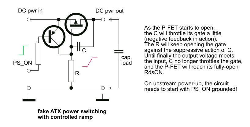
Let me start a little off topic, with a principally simple idea of how to
bias a power MOSFET with an RC circuit at its gate, to result
in a linear slope. It's really a simple case of a negative
feedback, voltage-coupled.
The example circuit is off topic here, because it's not useable
for our "auxiliary inrush limit" scenario.
It is relevant in the sense that it provides controlled
switch-on with a gradual charge balancing between two power
capacitors, using a linar feedback-controlled MOSFET
= it does show some direction.
Apart from requiring an external control signal, this simple topology has the following disadvantages:
I've actually used the "fake ATX" circuit in practice in one of my DIY prototypes (in a low-watt HTPC PSU).
The following circuit only exists as a simulation.
I've never built this in practice. And, the simple
simulator toy at falstad.com, while beautiful,
sometimes struggles to "converge". But, in principle
it appears to work as designed.
Click for a larger full-screen version of each picture.
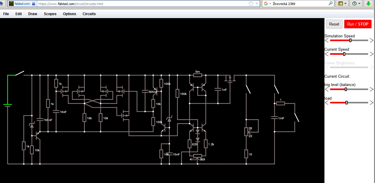
Inrush limiter circuit, pure schematic
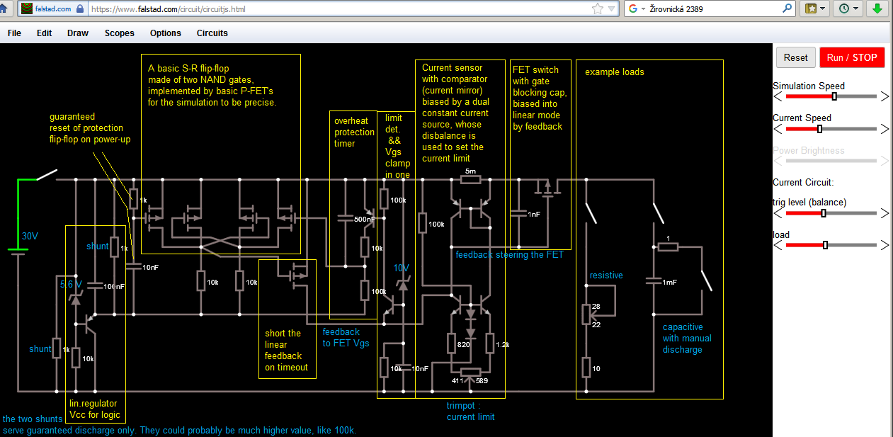
Inrush limiter circuit, with comments painted in
Source code of the circuit in falstad.com format is also available. Hard for me to tell for how long it will remain compatible with the simulation engine.
Note that this circuit actually limits the current through the FET
to a constant maximum value (rather than carve a strict voltage-based ramp)
and puts a timer-based limit on the maximum duration of the "current limit" state.
Plus, the timer does not reset when the "limit condition" is left for just an instant.
The timing capacitor takes time to discharge.
The circuit also works during later runtime, as a current limiter
with a time limit - effectively a soft and patient circuit breaker.
Once the timer kicks in, the only way to reset the circuit is by
a power cycle on its input.
When in operation, the FET dissipates heat. As long as the start-up period is short, either because the load capacitance is small, or the timer is set short, the FET probably does not need a heatsink. Its own thermal capacity should be enough to absorb the inrush energy. Pending practical verification :-)
It may have dawned on you already that I'm a fan of this analog poetry.
If you're curious where I come up with these curious all-discrete topologies,
check out an excellent free book by Hans Camenzind called
Designing Analog Chips.
Hans was a prophet, if not one of the founding fathers of the silicon industry.
I've actually discovered this book pretty late (2018-ish), and I have
decades of previous scattered reading and DIY on those topics - but Hans'es
book neatly summarizes the basic principles and building blocks.
Notice how I (ab)used a traditional current mirror as a high-side
differential input stage around the current sensing shunt resistor.
An unorthodox differential input, making use of the inherent
very low impedance of the input voltage signal, allowing for a
"common base" input to be used, otherwise a current mirror
that's getting slightly offset by the voltage emerging
on the sensing shunt. Counter to that current mirror,
I've put a pair of identical current sources (rather than
just resistors, to maximize the voltage gain of the circuit)
with the balance between those current sources being adjustable
by a trimpot. To set the threshold / limit of the current
sensor, the trimpot at the bottom allows you to counter the
imbalance introduced by the current sensing shunt.
In practice the circuit would require some calibration on
a prototype and possibly on an individual piece, and the
"differential pair" transistors should better be matched
(picked for equal Hfe in the pair).
Given my mediocre knowledge of this stuff, this circuit
feels like a neat practical gag - although I suspect
that there's prior art, so my authorship is likely dubious...
If someone wanted to build this as an academic exercise, I suspect that some values of resistors / bias currents would use validation for heat dissipation, especially at higher nominal voltage levels (48V).
Again, this circuit only exists as a simulation. I'm wondering if it would make sense to have this manufactured as a commercial product.
So... is this the end of my story?
Actually, it's not.
A while ago, in one particular model of a computer, I have discovered a gem of wisdom: a linear current-limiting circuit with a FET, controlled by a dedicated analog IC ! It's small, its component count is low, it's nifty.
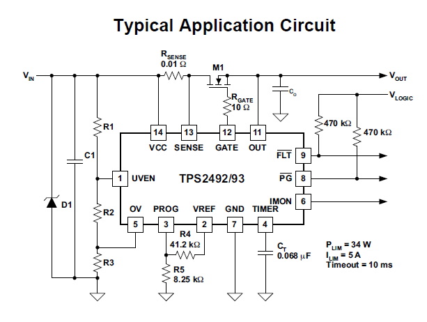
TPS2492 typical application circuit - from the datasheet
As it turns out, there's a category of power management chips called "hot-swap controllers". Their original intended use is for various industrial or telco electronics chassises, consisting of a backplane and insertable blades (adaptor cards), where the application favours a "hot swap" of the blades into the chassis, at runtime while the box is powered and fully operational. This is a scenario where you want minimal disruption to the internal low-volt DC power supply rails upon insertion of a blade into the chassis, so that the cards that are already in do not hang due to a power glitch. The hot-plug power manager chip's role is to softly attach the board just inserted to the chassis power supply rails and only then release the board for some internal power and reset sequencing.
Note that the TPS2492 drives an N-FET (my own circuit above contains a P-FET). This has consequences: the N-FET needs a positive gate voltage. I.e. the TPS2492 must provide a voltage above the Vin/Vout voltage level! The chip apparently contains an internal charge pump circuit to achieve that (no external capacitors, as far as I can tell - my respect.) Not sure exactly why the design engineer at TI has chosen an N-FET over a P-FET - it may have something to do with the fact that the TPS2492 also uses the FET for overvoltage protection. This is where the Vgate would not need to exceed the nominal limit, yet the FET's Drain could be allowed to float up... not sure about the Vcc and Sense inputs though, as well as the whole input section passives.
There are actually two sibling chips: the TPS2492 and the TPS2493. The only difference appears to be their style of recovery after fault: the TPS2492 stays latched, the TPS2493 tries again.
This is already pretty cool. Low component count, and verified in practice. The TPS2492 costs about 4 USD from Mouser. A suitable MOSFET would not be very expensive either. Obviously the maths are not as straightforward for computer makers, where cheap models are pretty constrained in terms of the BOM / budget. In my eyes, wherever I meet this chip, I can see attention to detail.
The one thing that's still missing is: bulletproof polarity reversal protection. Actually it's no rocket science either... But it's a topic for another paper I guess.
This scribble by: Frank Rysanek (rysanek [AT] fccps [dot] cz) (8/2020)