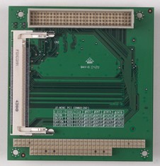
Click for a full-size image: [GIF] [PDF]
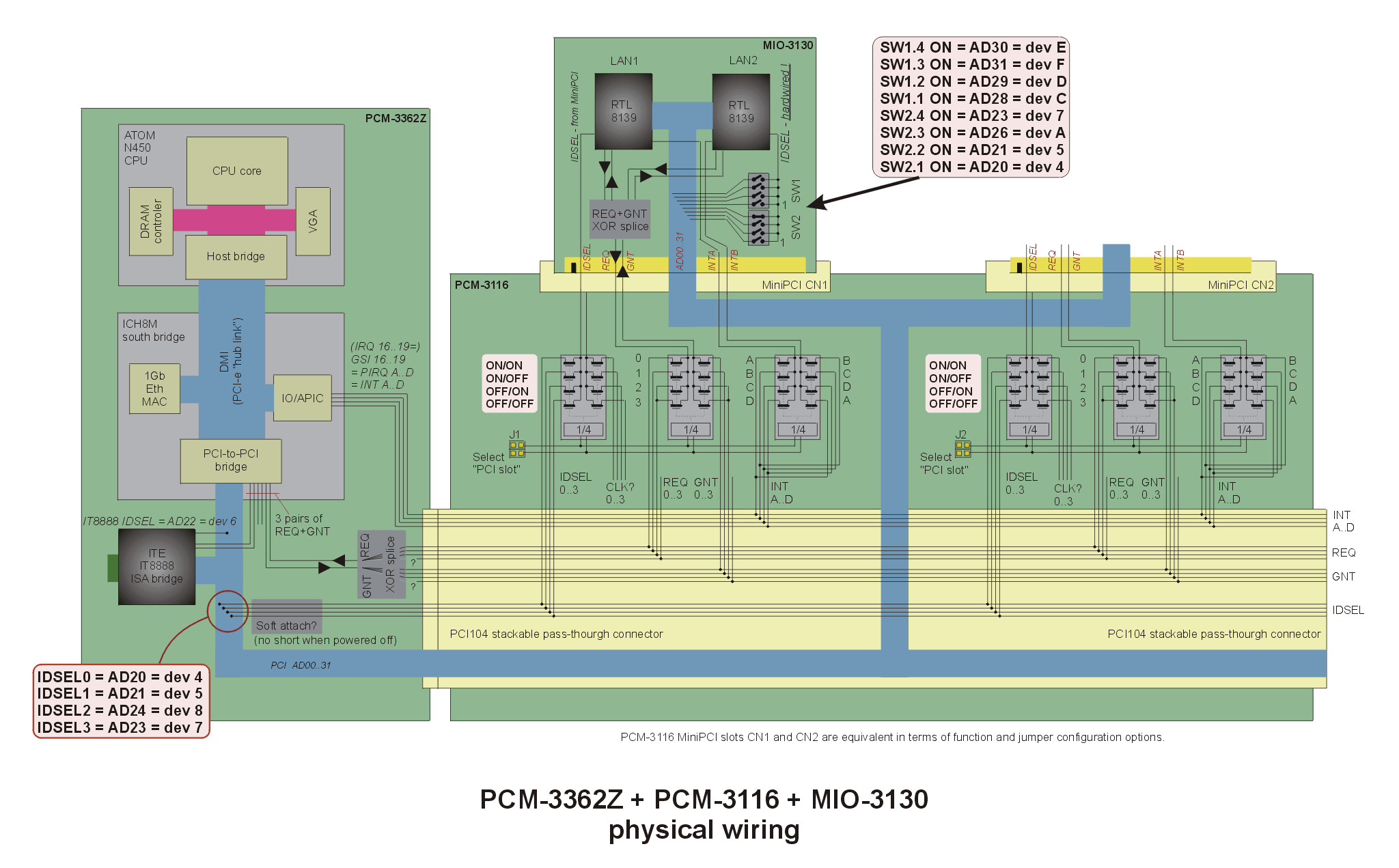
I work as a troubleshooter with a distributor of industrial/embedded PC hardware. It so happend, once upon a time, that I was asked to debug a particular PC/104 setup, consisting of some Advantech boards: the PCM-3362Z motherboard, the PCM-3116 "PCI104-to-2x-MiniPCI" almost passive conversion board, and the MIO-3130 dual-port MiniPCI LAN.
Enough of void talk, let's start with a picture to get you interested :-)
Click for a full-size image: [GIF] [PDF]
The following is a table of possible vs. valid combinations of jumpers and DIP switches, originally "brute forced" (walked through) on physical hardware. It was only after I filled in this table that the various pieces of the puzzle (background principles/rules/restrictions) started to snap into place in my head.
Click for a full-size table: [GIF] [XLS]
For datasheets, manuals etc. check out the Advantech web sites mentioned in the references. The product-specific links are dynamic and do change now and then. The fastest way of navigating to products is using the websites' keyword search (enter the bare product name).
This PC/104 motherboard is based on Intel ATOM N450 CPU, somewhat unconventionally combined with the mobile ICH8M, instead of the usual ultra-low-power NM10. The DMI hub link sure allows for that cross-over solution. The reason for this cross-over is likely the higher numbers of peripherial ports available from the bigger ICH.
Apart from the Atom "CPU" and the ICH, the board contains a classic IT8888 PCI-to-ISA bridge by ITE, used to provide the legacy ISA signals to the PC104 connector, an SCH3114 LPC SuperIO chip by SMSC, providing serial ports, PS2 KB+mouse etc., an Intel 82567V GbEth PHY etc... (including an onboard 2GB SATA flash drive, wow!)
Note that the ICH8M provides 3 channels of REQ+GNT,
but it would seem that 1 channel out of those 3 goes to the
IT8888 - at least that bridge does have the corresponding pins.
I'm not entirely sure they're mandatory, if the IT8888 isn't
allowed to perform legacy ISA DMA anyway (the ICH south
bridges from ICH5R above lack some further signals
needed for that, PPDREQ+PPDGNT I guess).
Anyway - I mean to say that mere 2 channels of REQ+GNT
are not enough to support the 3 independent REQ+GNT
channels that seem to be present in the PCI104 connector.
So either there is some Advantech-proprietary secret
sauce XOR-like splicer for REQ+GNT on the motherboard,
or all 3 REQ+GNT signals of the ICH8M are wired to PCI104.
The onboard IT8888 also occupies an IDSEL linked to AD22
(PCI device #6 on the relevant bus #1). The AD22 is therefore
not available for PCI104 IDSEL2 (this is instead wired to
AD24 = device #8).
This choice of IDSEL for the ISA bridge seems a tad unexpected
by the PCM-3116, but likely expected by the MIO-3130 (no secondary
IDSEL mapping for device #6 nor #8).
There are no further onboard parallel PCI devices,
i.e. no further IDSELs and REQ+GNT channels occupied
on PCI bus #1.
All the other onboard (on-chip, really) PCI devices
are dangling off logical PCI bus #0 = straight off the
DMI "hub link" (really looks more like PCI-e).
That applies e.g. to the integrated HD Audio interface,
USB controllers, GbEth MAC, individual PCI-e ports
(each has an inherent individual PCI-e device with IRQ
to signal hot-swap events), the LPC bridge etc.
The PCM-3662 motherboard by default has the VI/O pins in the
PCI104 connector jumpered to its internal +3.3V power rail
(generated by the motherboard). This happens to be contrary
to the manual (which claims +5V default for JP4) but that's
the way it is.
This default may lead to an ugly collision (short circuit) with some
3rd-party PCI104 daughter-boards that may hard-wire the VI/O pins
to +5V instead. (Happend to me, the motherboard survived.)
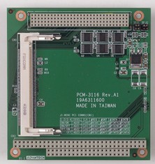
The PCM-3116 is a daughterboard in the PC/104 format, serving as a conversion board from PCI104 to two MiniPCI slots.
The two slots have an identical set of possible configurations.
You have to take care to jumper each slot for a different PCI
slot ("row in the table"), otherwise the two devices collide
on the same idsel and will fight for the various bus singals
already during bus init.
But if you only use a single MiniPCI slot (the other slot
remains empty), this is a non-issue, as the FET switches
are essentially passive (true "electronic jumpers").
Job well done on those switches - this style of jumpering
doesn't allow you to select illegal combinations
of IDSEL+IRQ (= combinations other than those expected
by the motherboard's IRQ routing tables).
The PCM-3116 provides its own +3.3V to the MiniPCI slots (also hardwired to +3.3V "aux" = 3.3VSB.). That output 3.3V power rail is generated using a linear stabilizer from the input +5V rail (from the PCI104 connector). I.e., the PCM-3116 won't draw power from the motherboard's 3.3V power rail (possibly generated by the motherboard itself) present in the PCI104 connector from the motherboard.
The VI/O pins are passed through, not connected to any particular power plane (not even to each other).
Note that as of the time of this writing, the silkscreen table and the manual both map the per-MiniPCI-slot IDSEL straight to the motherboard's AD20..23, which is inappropriate, and in the case of PCM-3362 it is wrong about AD22 (really AD24). If the docs would instead refer to PCI104 IDSEL0..3, that would be precise. When in doubt, refer to my table and pictures presented here.

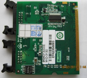
The MIO-3130 is a dual-port FastEthernet card in the MiniPCI format. The interesting question here is, how the hell did they combine two distinct and identical PCI NIC chips (PCI devices) onto a single MiniPCI board (a single PCI device per definition). Did they weld them together somehow, to make them respond as two different functions within a single device? Certainly not, these are plain bread'n'butter Realtek NIC's and do not have such a capability.
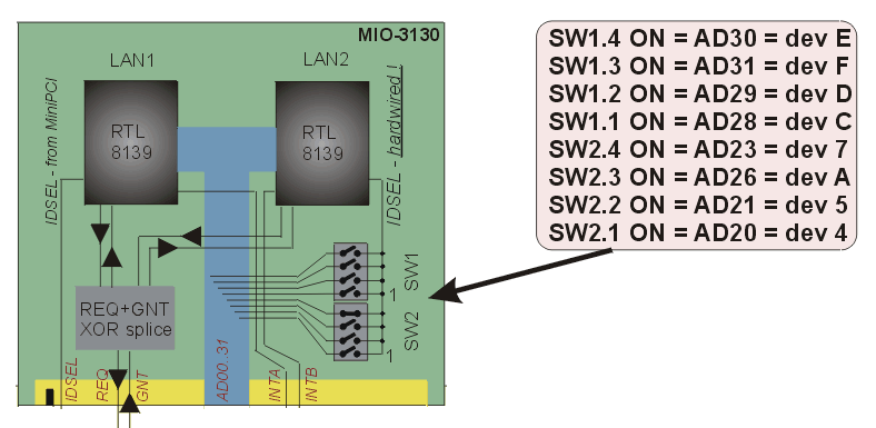
To understand the board's twisted tricks (and the implied pitfalls), you need to understand a bit about what makes a proper PCI slot (and MiniPCI slot).
The PCI/MiniPCI slot has a single IDSEL input, which is enough
to identify precisely one PCI device. This takes care of the port
labeled LAN1.
However, the IDSEL input pin is really just an external short
to some particular ADxy PCI bus line.
In order to make another PCI device appear on the PCI bus,
all you need is to hijack another ADxy line in the role of IDSEL.
Using the DIP switches, the board allows you to select one of
several ADxy lines for the secondary IDSEL, thus making the
secondary device (LAN2) appear as one of several PCI device
numbers on the relevant bus.
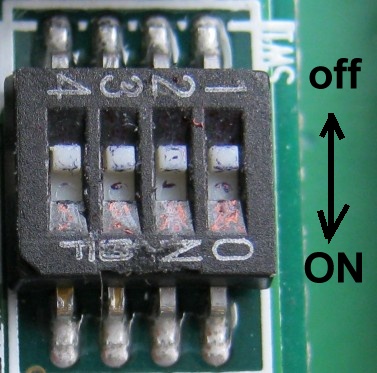
Note that there are two banks per four DIP switches,
each bank on a different side of the board. At a first sight,
it makes you think that each NIC has its own IDSEL selector
per 4 switches.
That is not the case though: both the DIP banks are related to NIC2
and you can simply view them as a single 8way DIP bank.
Only a single switch at a time can be "ON".
If you leave all DIP switches in the "off" position, you'd expect LAN2 to remain disabled. This is not entirely true though: the MIO-3130 thus configured makes the PCM-3362 hang during POST in some circumstances / for some reason. It really looks like some stupid bus collision, with some analog aspects (temperature dependence, power supply style AT/ATX). Once you select some non-colliding IDSEL, even if it doesn't obtain an IRQ, the machine boots just fine...
The MiniPCI connector conveniently provides two IRQ signals - these can be used directly for the two distinct PCI devices (NIC chips). There is a gotcha though: normally the second IRQ link would be an INTB on the primary PCI device. If we route it to the secondary PCI device (LAN2), it becomes the LAN2's INTA, and we have to make sure that the secondary IDSEL (PCI slot) has an entry in the BIOS IRQ routing tables, specifying some PCI IRQ link for the slot's INTA, and that the secondary slot's INTA is the same link as the primary slot's INTB (= few IDSEL's satisfy both rules). See the chapter below for broader theory / context (look at the picture).
Another interesting aspect is: how are both NIC chips
(PCI busmaster devices = relying on PCI DMA for data transfers)
able to work fine using just a single channel of REQ+GNT?
They certainly cannot share the REQ+GNT by plain parallel connection
- that would be an ugly conflict and both LAN ports would be defunct.
It turns out that all it takes is just some fairly simple logic device,
which OR's the REQ signals and makes sure that only one PCI device
at a time gets the GNT back (if they ever try to request
master access to the bus both at the same time).
There is some unidentifiable chip on the flip side of the board
which appears to perform this "XOR splice" function - that's where
all the REQ and GNT signals meet.
The common ADxy signals used for PCI payload transfers are simply attached to both NIC chips in parallel, no problem there.
The PCI bus tree works with a fairly simple device addressing key:
the bus:device.function triplet.
For most practical purposes, "PCI device" == "PCI slot" (they are synonymous)
- although it needn't be strictly a mechanical connector, it can indeed be
an onboard device. The point is that a single device (or a well-behaved slot)
is addressed by a single IDSEL signal (like a "chip select"). The upstream
bridge could have a dedicated IDSEL signal for each supported slave device#
- but for practical/efficiency reasons, the IDSEL signals are actually
mimicked using the bread-and-butter ADxy signals (Address and Data,
32 of them in a 32bit bus). This alternative use of ADxy for IDSEL
has been a part of the PCI standard for ages.
IDSEL's are only needed during bus configuration, so this substitution is
no problem (no conflict during routine operation later on).
In routine operation, individual devices respond to IO addresses spotted on the PCI bus
(using programmable address decoders, that have been set up during configuration phase).
The generic PCI algorithm of bus enumeration using IDSEL's and the establishment
of non-overlapping IO and IOMEM windows are a part of the PCI standard.
This is done on every BIOS POST (or maybe every OS boot, if the OS elects to
do this itselfs).
The bus is a single metallic segment, ruled by its closest upstream PCI bridge.
In this PCI104 case, our PCI104 is bus number 1.
You can also have semi-virtual busses, emulated on top of more complex
infrastructure - such as, the whole "hub link complex" from the host bridge
(north bridge) to the south bridge, hosting all the chipset's on-chip PCI
devices, also amounts to just a single logical PCI bus (number 0).
The PCI bridge between busses 0 and 1 is a part of the ICH south bridge.
The "function" is a subsystem within an addressable device =
all the "functions" within a parent PCI device share the parent device's IDSEL,
and typically they are on-chip subsystems of a single common chip (such as,
two ports of a dual-port SCSI HBA or a dual-port Eth NIC chip).
Otherwise though, at runtime, from OS perspective and driver instance perspective,
they work as pretty much independent PCI devices. Each function has its own PCI config
space etc. An outside sign of this is that most PCI scanning utils (such as the Linux
lspci) list them as separate full-fledged rows/entities in the table of devices.
It is sometimes said that each function can use its own IRQ (INT signal)
from the parent device's "PCI slot" - but I don't think the mapping needs
to be strictly 1:1.
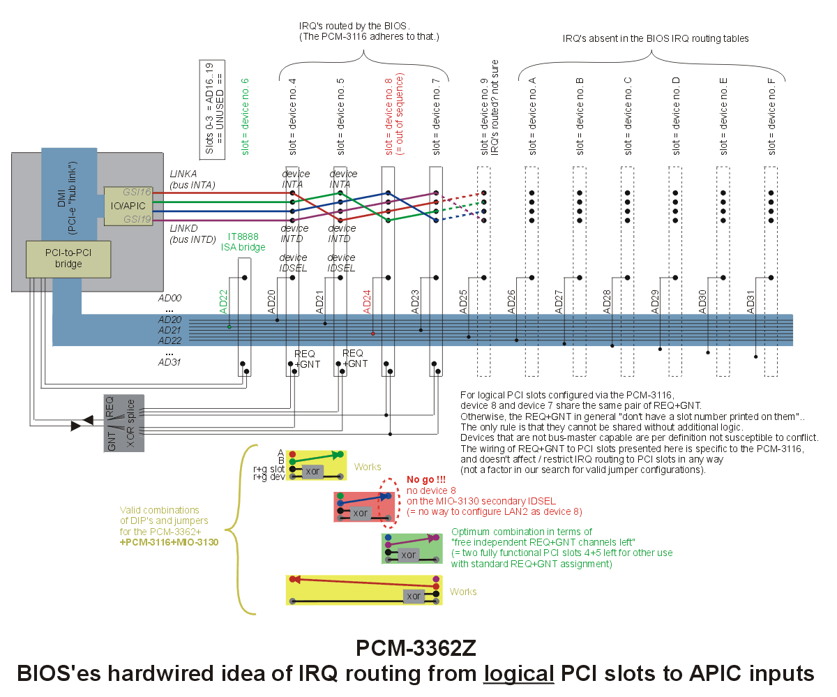
Click for a full-size image: [GIF] [PDF]
The logical topology sketch above has one primary purpose: to show the basic idea the BIOS has about IRQ routing to individual PCI devices. For a start, please focus on the four interrupt links going from the APIC to the set of PCI slots supported.
Especially note the swizzled braid of interrupt links
- this seems to be the trademark idea of sideband
IRQ routing alongside the PCI bus, appearing in any
PCI bus tutorial.
Next, note that the braid swizzling algorithm
is not exactly set in stone. It is generally applied
as mentioned in the standard, but the motherboard
designer has the freedom to set up custom optimizations
/ anomalies as required by his set of onboard devices
and expansion slots. E.g., in our case, note how slot #8 is
inserted in the "IRQ braid" at a position where you'd expect
slot #6.
As a result of historical evolution, there are several BIOS
subsystems / API's / tables that can provide a modern OS
with IRQ routing information. The precise IRQ routing
topology is a matter of motherboard design. The final
design gets reflected in the IRQ routing tables,
and is fixed => the interrupt routing
is NOT established dynamically by probing at every
POST or during OS boot. There's no generic PCI config mechanism
for establishing the IRQ links! The IRQ number stored in the
per-device PCI config space header is just a "scratchpad variable"
filled in by the BIOS or OS based on its tables. There is no generic
way to trigger a dummy interrupt via PCI config space of a
particular device and see which GSI fires on your APIC's.
Hence an OS can hardly infer anything
on its own on a hardware setup that has the BIOS IRQ routing
tables flawed (deviating from hardware reality).
The various IRQ routing tables provided by the BIOS
should match each other (at least in some "common
denominator subset"),
so it shouldn't matter much whether you take your
APIC IRQ routing information from MPS or ACPI.
As far as the "generic braid" goes, it appears that modulo-four
PCI device 0 starts with "device INTA" bolted to "PCI bus IRQ link A".
Each PCI device can have up to four INT pins
(connect to up to four of those PCI IRQ links), and the actual usage
of per-device INT input is stated by the PCI device's config space,
so the system knows which pin(s) it has to look up in the
BIOS tables. In addition, in our case, note that:
A side note on PCI Device #6 (slot #6) = the IT8888 PCI-to-ISA bridge:
the bridge doesn't use an IRQ of its own. Rather, the ISA bus has its own set
of IRQ links, attached to a dedicated set of ICH inputs = the legacy AT PIC inputs.
The IT8888 is responsible for decoding the ISA IO and IOMEM address ranges,
not for the interrupts.
An interesting aspect of this ISA bridge is that when combined with Intel-based
system chipsets, this bridge is "invisible". Probably "hidden from view" by the
BIOS during POST. Makes me wonder why it remains normally visible on Geode chipsets.
Also, with Intel chipsets the IT8888 address decode windows tend to get configured
automagically, whereas on Geode-based systems you have to configure the decode
windows manually in the BIOS Setup to suit your needs.
There may be some technical reason to those differences, or it might be a matter
of software licensing (the automagical configuration module for the BIOS
being only available from Intel with its chipsets).
The basic read/write operations on the PCI bus are those coming from
the host CPU (or root complex).
On the PCI bus itself, they are initiated by the host bridge.
They consist in basic polling access for a single byte/word/dword.
Configuation access is similar.
None of those transactions need "bus mastering" - the peripherial
device is always a passive "slave", only responding when asked.
The signals called REQ and GNT are only needed for bus-mastering operations = when the peripherial device wishes to start a transaction on the bus, rather than the relevant upstream bridge. The typical (only?) use for this is Direct Memory Access (DMA). Bus-mastering and DMA are almost synonymous on the PCI bus.
It works like this: when a device needs to write (or read) something via DMA, it asserts its REQ (request) signal. The upstream PCI bridge can see that, and when it's ready, it asserts the corresponding GNT (grant) signal. The device then performs its transfer (as configured in advance by other means). When the transfer is over, the device releases its REQ, and the bridge releases the corresponding GNT. (The peripherial device then perhaps informs some software running on the host CPU via an IRQ, but that's a different story.)
The REQ+GNT signals tend to be a "scarce resource" on the various PCI
bridges, especially those integrated in PC platform south bridges.
There tend to be only a handful of discrete REQ+GNT "channels"
(say 3 to 6, but some ultra-mobile chipsets may be down to 2).
In the chipset and PCI104 connector pinouts, the REQ+GNT signal pins
are "numbered" - but in reality they are all equal, they do not
address a particular PCI slot=device in any way. There's no
"DMA channel-to-slot" mapping table, as there's no need for
such a mapping. First come first served - you don't need to know
who it was.
When combining wild hardware setups, where you mess with the wiring of PCI slots and their various support signals (read: when assembling a PCI104 stack), you may find yourself short of discrete REQ+GNT channels. You cannot just hook up bus-master devices in parallel to a common channel - that wouldn't work. So... is there some way to multiplex several devices on just one BM channel from the chipset?
Yes, it is possible. It turns out that all it takes is just some fairly simple logic device, which OR's the REQ signals and makes sure that only one PCI device at a time gets the GNT back (if multiple devices ever try to request master access to the bus at the same time).
At the bottom of the "logical wiring diagram" above, you can see my attempt at graphical representation of the three valid jumper+DIP combinations for our example PCI104 stack. The arrow depicts the "hijacking of INTB to the neighboring slot's INTA" done by the MIO-3130, and the grey box is the REG+GNT splicer on the MIO-3130.
It really all started by the customer calling in, claiming that his pilot hardware setup (several pcs) showed weird symptoms - on occasions, it was refusing to boot in ATX mode, just hung before completing POST (no VGA, no beep). And it took a power-cycle and precise sequencing of the ATX power rails and signals to get it to boot. And it was completely refusing to boot in AT mode.
So I took the PCM-3362Z motherboard and had it up and running within minutes, in plain AT mode. I took care to test several PSU's with different "rise times", varying from 0.2 ms to 25 ms. The customer produced a neat oscillogram, showing that his rise time was a nice 10 ms.
Knowing that the customer does his own "ATX power-up emulation",
I went into some ugly detail in researching the precise behavior of the motherboard's
"auxiliary ATX connector" CN23 (having PS_ON and +5VSB for ATX mode, or just a jumper for AT mode).
I noted that, unlike PICMG motherboards, where the jumper shorts +5V"AT" to +5VSB
(the center pin is +5V"AT"), on this PCM-3362Z the jumper shorts +5VSB to GND
(the center pin is ground).
Probably some bootstrap, telling the motherboard to handle/feed +5VSB internally.
I also noticed that PS_ON was active even when jumpered for AT mode, and could be used
to detect proper graceful shutdown of the host OS (internally, the motherboard still
provides the ACPI/APM API's for software-driven power-off).
I also noticed an interesting behavior where, if you removed +5V"AT" power at runtime,
while keeping +5VSB up (without a proper ATX software-driven power-down),
the machine would keep running on just +5VSB, and would even feed some juice
back to the +5V"AT" power rail, back to the PSU :-) It took a beefy +5VSB rail,
capable of 2A+ to keep the board going... and it proved completely fruitless,
this was not a problem by our customer.
The customer took his turn investigating this train of thought, and confirmed that
indeed his motherboard alone (no PCI104 peripherials) does boot just fine and rock solid,
even in AT mode.
And went on to point out that it's only the completed PC/104 stack that misbehaves.
And, found out that the misbehavior was somewhat temperature-dependent. That the machine
was more likely to fail to boot at very low temperatures (say below 10oC).
Yet the temperature dependence only showed in the complete stack, he reported.
You could freeze the bare motherboard down to -20oC and it would still boot
just fine.
He also pointed out that he didn't quite know what to do with all the jumpers - specifically
on the MIO-3130 MiniPCI 2xLAN daughterboard, but also on the PCM-3116 conversion board.
And that he basically just kept the defaults (jumper combinations).
We quickly tested that the motherboard alone did boot just fine over a wide range of
temperatures, thus excluding a problem with some "health monitor temperature limits"
playing hide-and-seek with us via the BIOS (seen that before). So the temperature
dependence of the symptoms, while positively existing, was probably pure coincidence
/ side effect of some deeper problem.
And, we verified that the whole stack fails to boot in AT power mode.
I noticed how the PCM-3116 "almost passive" conversion board was making its own +3.3V from the +5V"AT" provided by the motherboard. And that the resulting 3.3V rail was rather starved of filtering capacity. I tried adding some filter capacitors, which had no effect whatsoever.
Finally, I went on to compile a "PCI bus map" from various sources. I knew right from the start this would be appropriate, and was looking forward to the job, only somehow I tried other possible causes first... (see an "analog" problem, try some "analog" explanations / remedies first).
So: there I was, trying to figure out how the various ADxy, IDSEL, REQ+GNT and IRQ/INT[ABCD] wires played together in the complete stack. And I quickly realized that the documentation was rather sparse. I also knew from the start that the two Realteks on the MIO-3130 would be unable to run DMA properly on just one set of REQ+GNT (or would they?) and just one IDSEL signal (so I wasn't surprised to find some IDSEL/ADxy mapping jumpers on the MIO-3130). Later it dawned on me that it *was* possible to multiplex several PCI devices onto a single set of REQ+GNT with relatively simple XOR-style logic - but I was very suspicious about the timing capabilities and propagation delay of that micro-FPGA-or-what hack of a chip, added by Advantech to the MIO-3130 to implement that functionality. I smelt a rat right there, and I have to say I was wrong :-)
Using other clues, I managed to build the map. I started by reading the
relevant chapter of the ICH8M datasheet, specifying how ADxy in the role of
IDSEL's mapped to PCI device numbers on the 32b PCI bus.
Using an ohm-meter / short indicator, I also tracked how the PCM-3116 jumper
combinations mapped to the individual PCI104 IDSEL and IRQ signals.
The next semi-tough part was to find out how the motherboard mapped the
ADxy to PCI104 IDSEL[0-3]. As the signals are not hard-wired together
(rather, it seems like the motherboard switches them together electronically),
I had to find out by experiment. I used some basic MiniPCI WiFi daughtercard
and tried all the four combinations available from the PCM-3116 conversion board
- and I watched the PCI device numbers reported by Linux (or DOS-based PCISCAN)
and derived the corresponding ADxy from the PCI device number: AD# = PCI_dev + 16(dec).
The toughest part was to figure out, what the MIO-3130 DIP switches actually meant.
The table in the manual was both cryptic and wrong in some respects. Initially
I thought each DIP bank (SW1, SW2) corresponding to each LAN port (LAN1, LAN2).
I first tried iterating through all binary combinations of SW1 (with SW2 all off),
then all combinations of SW2 (with SW1 all off). That's 16+16 combinations.
Initially I was looking for combinations where both Ethernet NIC's were
visible on the PCI (these weren't many). Interestingly to me at the time,
combinations of "promising SW1 vs. promising SW2" didn't work out at all,
despite the fact that the IDSEL mappings they manipulated didn't overlap.
An interesting observation at this stage was, that any combinations yielding
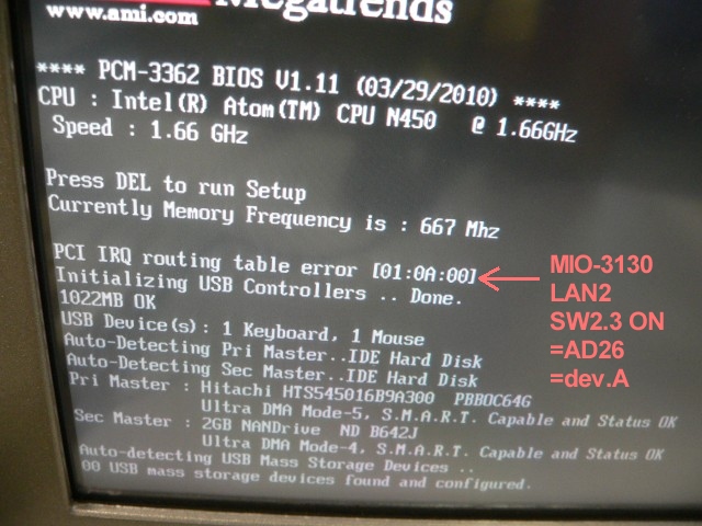
two visible Ethernet devices would boot just fine in AT mode - and I suggested
one to the customer, who immediately confirmed that the "hang during POST"
was gone. But the second port, although visible as a PCI device, was still
defunct, apparently due to a defunct IRQ or bus mastering.
Next I took a hard look at the combinations collected so far, and I was
starting to "see a pattern". When I put the two DIP banks "side by side"
in one big table, and used some other clues to tell which physical NIC chip
corresponded to which IDSEL, it dawned on me that both the two DIP banks
manipulated only the LAN2 IDSEL (I had a choice of 8 IDSEL's total),
and that LAN1 was staying put at "PCI device #5" in my case. And that really
just a single DIP switch out of the 8 DIP's total should be ON for a valid
DIP switch combination. That's 8 valid combinations total.
An interesting side-effect of all the illegal combinations that I tried was,
that occasionally I collided with something at AD22 IDSEL (PCI device 6).
The device ID was always something like 0888 or 8080, and the vendor ID
was always "ITE" => I was clearly running into the on-motherboard IT8888
auxiliary PCI-to-ISA bridge :-) If I invalidated its device ID, the BIOS
would fail to hide it from sight during POST.
It was fairly obvious to conclude that MIO-3130 LAN1 uses the standard
dedicated MiniPCI IDSEL - which in turn would be assigned by the PCM-3116
"jumpered slot".
And another pretty tough part turned out to be to figure out what jumper
combinations would yield a working IRQ setup. Again, by the random attempts
so far, there wouldn't be many, if any at all. At this point I knew that
I had 4 valid combinations on the PCM-3116, vs. 8 valid combinations
on the MIO-3130 - giving a total of 32 combinations. So I decided to build
a table and try all 32 combinations. And, I had to test all the promising
candidates in Linux, by actually trying some load (outbound ping).
Sending packets back'n'forth is enough of a proof that both IRQ and
PCI busmaster DMA work right. The DMA was always allright, the IRQ's
were definitely not :-) My "exhaustive iteration" was greatly sped up
by the fact that with many combinations, already the BIOS reported
an "IRQ routing error" straight after POST - so I didn't have to boot
into Linux to investigate further. In several other combinations though,
two IRQ's got assigned, but the second IRQ was undelivered or mis-delivered
(appeared on another GSI). In the end, only 3 combinations worked exactly
right! What ho?
By looking hard at the jumpering table, another pattern or rule might
start to dawn on you. Can you see the sequence in how the "second" IRQ
gets assigned? Yes, it's A/B/C/D "bottom up" - but some rows break
the pattern. If you look at the MIO-3130 direct-wired secondary IDSEL's
(PCI devices), and align them to the way the PCM-3116 assigns the primary
IDSEL's (PCI devices), and how the primary IRQ's correspond to primary
IRQ's, you'll notice that the mapping of
"secondary PCI device (IDSEL) -> secondary IRQ" follows the same
pattern. It appears that this is not by accident - so, exactly what's
the rule behind this?
It's the IRQ routing tables that are a fixed part of the BIOS.
See the chapter on Theory and Principles above.
In the beginning of 2011, this has been quite an unexpected adventure.
What a marvellous tour of PCI internals and other people's PCI hacks -
in an era when parallel PCI seems to be vanishing from desktop hardware.
PCI-e should save us all in no time. Or should it?
Considering that ISA is still alive and kicking, both in the form of
PICMG 1.0 and PC/104, I'd expect the classic parallel PCI to stay
with us for several years to come... It may withdraw from the mainstream
desktop, but it'll stay strong in our "industrial" niche, possibly
also in ultra-low-power consumer gadgets. The volume of PCI104 sales
does not exactly amount to making us a living, but the technical
gotchas are a lot of fun :-)