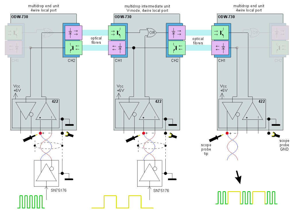
An example test setup - three pcs of ODW-700's, fed by two rectangle signals with different frequencies, OR'ing them together
By: Frank Rysanek of FCC prumyslove systemy s.r.o. [ rysanek AT fccps DOT cz ]
This writing exercise has been prompted by a particular field trip,
where I found out that I knew rather little about the "synchronous mode" feature
of the Westermo ODW series bus converters (RS232/422/485 over fibre optic)
that we sell where I work.
I was caught somewhat unprepared, but managed to help solve the problem on site
using an improvised test bench setup and an oscilloscope (and I owe many
thanks for the protocol-side part of our solution to a senior programmer
on site, Mr. Vladimir Jaros, our customer's subcontractor).
I then followed up in the lab, using a slightly bigger test rig
- essentially doing my long overdue homework.
And this paper is a compilation of my findings about Westermo hardware,
including some slightly offtopic aspects.
...an example test setup to attract your interest...
The topic is somewhat complex, and we have to start somewhere. Inevitably, it will feel like starting from the middle. And in my opinion, it is appropriate to start with an interesting picture and follow up with some theory for explanation, rather than start with all the boring theory and finally get to the point at the very end...
At this point you may be asking yourself, what the point is, why would anyone
want to transmit rectangular signals, and have them "OR'ed together" by the bus?
The point is to prove, that the sync mode can indeed transport arbitrary signals,
and moreover, it shows the precise behavior upon "collision" = when several nodes
start transmitting at the same time.
Note that the resulting output is indeed
a precise "OR" combination of the input signals in time. One could for instance
imagine, that the right-hand transmitting node could mask its left-hand neighbor,
perhaps subject to "turning time" etc. (not the case, as you can see).
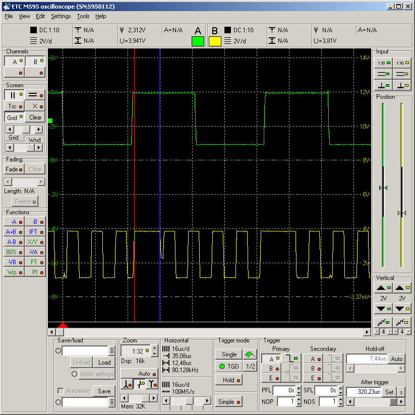
This is what it looks like on an oscilloscope (click for a bigger screenshot):
Input signals on the left side, combined output on the right
The middle unit is configured for "V mode"
- this is to make the sketch simpler (more obvious to understand)
and also to form a bus that's capable of full-duplex "4 wire" transmission
between the master node (on the right) and any particular slave node.
It was one of my objectives in this exercise, to verify that full duplex
is indeed possible without any non-obvious constrainsts (such as turning
time intervening somehow).
The "multidrop end units" don't really make a difference between V-mode
and Y-mode. In the ODW-700 series, the box configured as an end unit
automatically understands that whichever optical port becomes active
(linked), it is the one port to use - in Y mode it doesn't matter (both
ports are equal), in V-mode the box has to flip the V's direction if optical
CH1 becomes active (normally CH2 is the upstream port). In the ODW-600
series this had to be observed in the jumper configuration.
I have a simple dual-channel (dual-trace) USB-scope. Therefore I can watch no more than two signals at the same time. The RS485 wiring is balanced - so theoretically I can attach a single-ended probe between + and - (which is awkward, as it compromises the symmetry), or I can attach two probes with tips to + and -, and ground them both to the RS485 reference ground... In the latter case, I'd waste both probes on just one signal to watch - fortunately, apart from being ugly to watch, it's not really necessary, as under healthy circumstances, the two wires are indeed precisely complementary. Therefore I prefer to attach my scope probes to the "+" terminal on the RS485 line interface and ground them to the driver's reference ground (even if that's sometimes difficult to reach). That's why in my sketches and scope screeenshots, typically you'll see the RS485 level signals "normally low, with pulses active high" - that's aligned to the "Westermo polarity" (corresponds to the "+" label on the converters and to the OR gate being mentioned in the manual).
The schematic sketch above is technically incorrect in several respects.
For instance, the "+" labeled terminal on the Westermo box might possibly
be connected to the RS485 xceiver chip's nominally inverting pin on the inside
(not that it would matter much alone, except that the "OR" might be more like
an "AND"), and the true schematic, even at the block level, is a lot more complex
- the box supports multiple modes of operation that are logically quite different,
the optical links actually run a synchronous bitstream with a multiplex of different
data, there's reclocking going on between the optical ports, most of the logic
is embedded in an FPGA anyway etc.
The sketch is good enough exactly for your initial idea of the overall behavior.
The SFP's used in the ODW series are nominally designed for 155 Mbps synchronous clock rate (SDH STM1) - and the actual clock rate that Westermo is using will likely be in that ballpark. Over that clock rate, the ODW converters encapsulate their payload, multiplexed with some service overhead data (ring management, remote failure signaling etc). Based on some ODW-600 era information, the actual payload (input metallic signal) in synchronous mode gets sampled at 95 MHz. The ODW-700 support two virtual transmission channels (virtual busses) to coexist on a single physical infrastructure, i.e. they're mutiplexed, i.e. perhaps the actual payload sampling rate is now half the aforementioned figure.
At this point I can hear you murmur "...right, that's all very nice, but where does the "turning time" come into play? You've promised to tell us..."
In the eye-catching example above, the ODW's were configured for maximum possible turning time, which is 1.6 milliseconds. Hence, the turning time was set much longer than the longest period of constant level in our testbed signals - the slower rectangle was about 60 microseconds full cycle, i.e. about 30 us edge to edge. As a result, the RS485 driver was always on, never releasing the bus. That's why the oscillogram doesn't show any signs of the driver turning off - all you can see is logical zeroes and ones, both of which are active states on RS485/422.
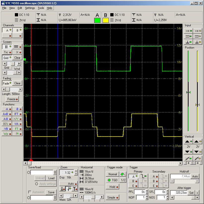
On the following pinout sketch, you can see the ultra-classic RS485 transceiver: the 75176. Note the input labeled DE (pin 3), which means "driver enable". If you feed this input a logical zero, the driver will turn off all its output switches (transistors), thus effectively releasing the bus into a high-impedance state. This is normally used in half duplex communications, to allow the other nodes on the bus to have their say.
DS75176 RS485 transceiver pinout
(the bus/line gets attached to pins 6+7)
Turning time has to do with the TX driver engaging and disengaging on the RS485 transmission line (signal pair) - and maybe it also has an internal meaning in the ODW boxes, towards the optical bus.
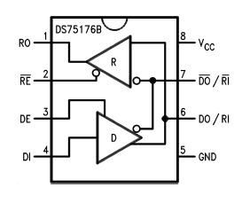
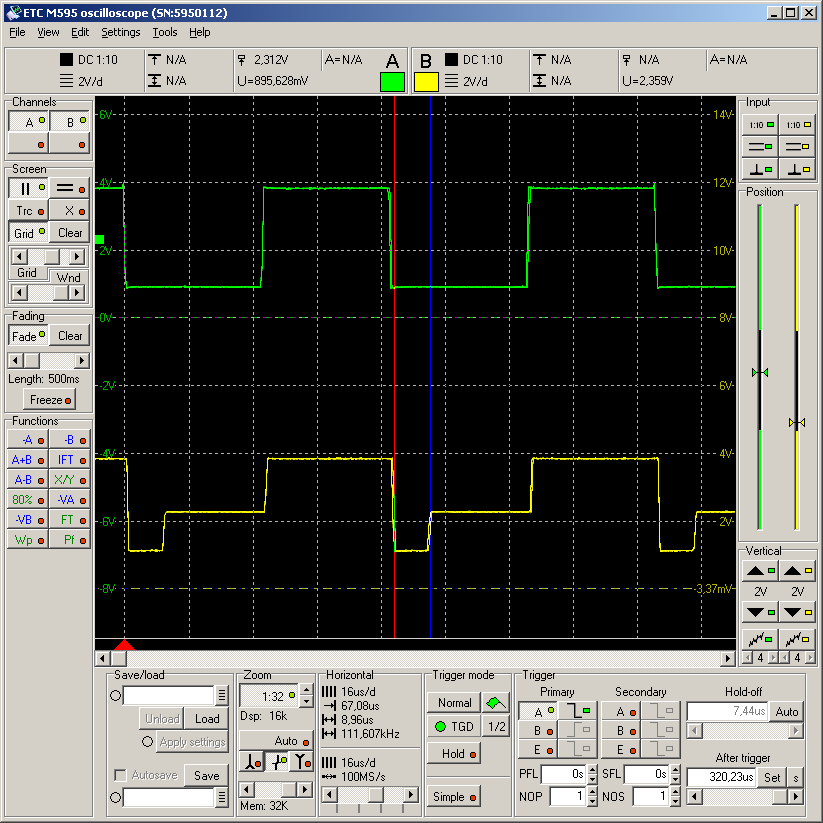
In the following oscillograms, you can see what happens if the turning time gets shorter (faster) than our payload signal. First there are three examples, where the input signal is a plain rectangle - our slower testbed signal (30 us edge to edge):
Basic 30+30us rectangle with 8.6 us of turning time
(green: input, yellow: output)
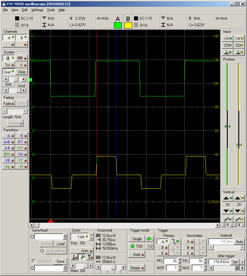
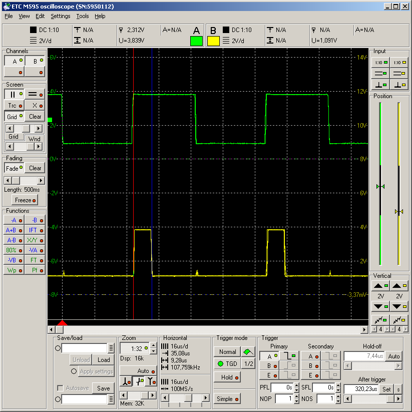
Basic 30+30us rectangle with 13 us of turning time
(green: input, yellow: output)
Basic 30+30us rectangle with 26 us of turning time
(green: input, yellow: output)
That seems fairly obvious, right? The time starts counting down
from the last edge in the payload signal - and the edge can be upward
or downward. It seems that the "turning" is some kind of a single-shot
circuit, that disables the RS485 driver upon timeout = this logic likely
resides within the "converter of destination", and every converter is
a destination for some direction, in a duplex system.
That's simple :-)
...or is it?
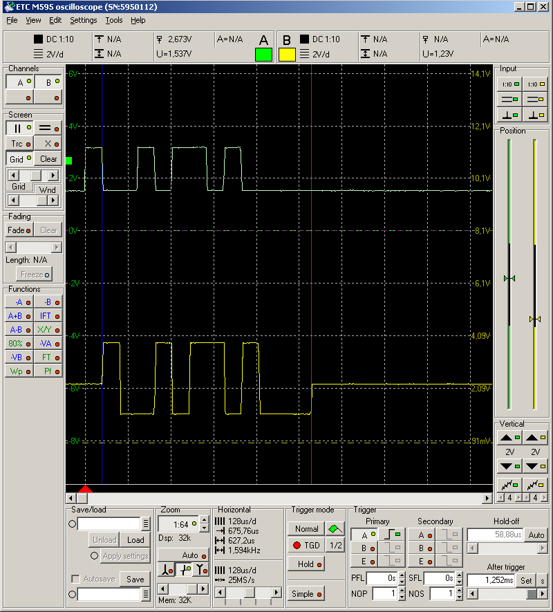
Upon closer observation, it indeed seems that the logic is not that simple. Take a look at the following screenshot:
Yes it's again our combined signal, from the very first sketch and scope shot.
Except that, because I only have a dual-trace scope, the scope screenshot doesn't contain
the faster input rectangle. But it does enter the mix.
This time, all the three ODW's in our test rig have been configured for 13 us
turning time. Can you see what happens? The turning time gets applied to the slower
rectangle, but not to the faster one. The physical RS485 driver at the destination ODW
does not actually turn off. As if the turning time was applied before
the OR gate in the middle ODW, in the form of a TTL "gate" signal.
And, somehow it only gets applied to the rising edge, not to the falling edge
(or perhaps we just cannot see). As if the "fiber optic backbone encapsulation"
did not transfer the "third state" (hi-Z), but indeed just logical one's and zeroes
(so that log.0 and third state are basically equal on the fibre optic bus).
It really seems as if the "turning/gating" was actually applied at two independent places in the transmission chain: using an "AND gate" on the local contribution towards the optical bus (at the source ODW), and using an RS485 driver to the local metallic segment (at the destination ODW). The turning signal (single-shot of some sort) is likely derived independently at each of those two places. See the following sketch:
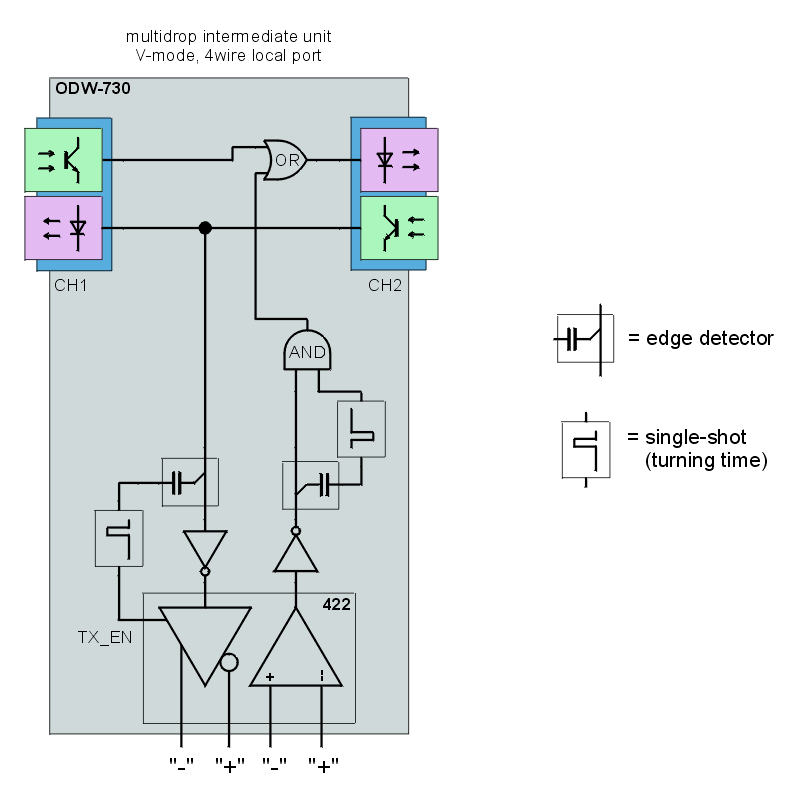
ODW-730 block schematic - including the turning single-shots
But wait, that's not all - there's more. You may be wondering along with me - if the two "places where turning time is applied" are independent, what happens if we set the turning time different at either end? Are we gonna get different turning behavior on rising and falling edges, respectively?
The resulting behavior may look weird at a first sight, as the two complementary
configs do not yield a precisely complementary result - but after some
thought, it makes sense, if you combine all the observations above.
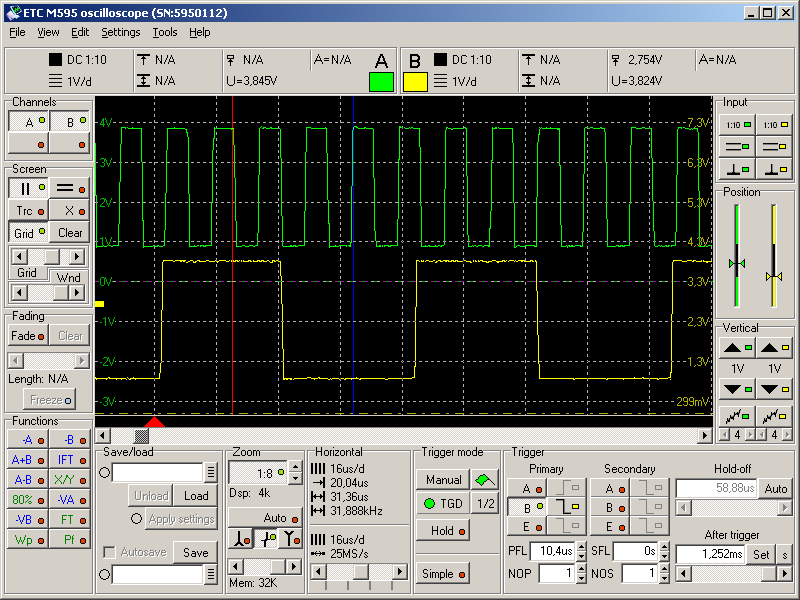
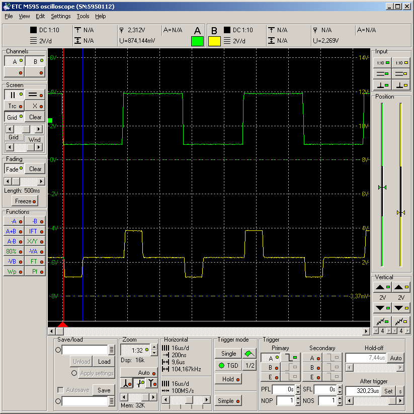
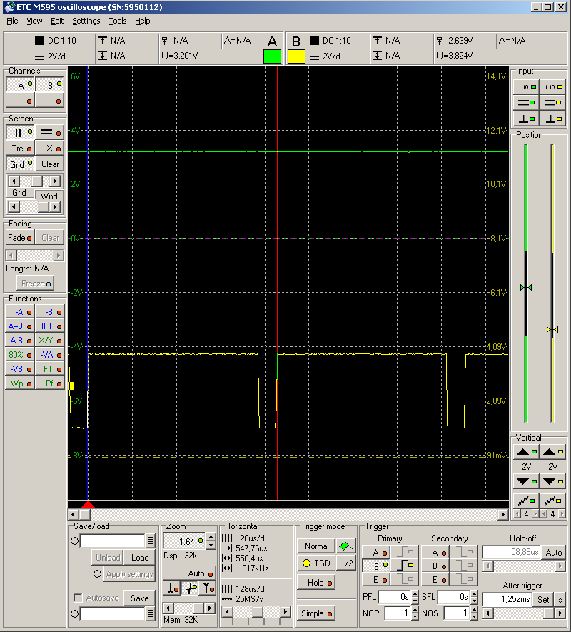
Take a look at the following two scope screenshots:
1.6 ms turning time at the source ODW, 8.6 us t.t. at the destination ODW
(green: input rectangle, yellow: output)
In this first example, the 1.6 ms timeout at the source ODW (= timer started by a rising edge) does not fire, as the input signal is much faster than 1.6 ms. The 8.6 us timeout at the destination ODW (= timer started by a falling edge) does fire - and because it's at the destination, it turns off the local RS485 bus driver.
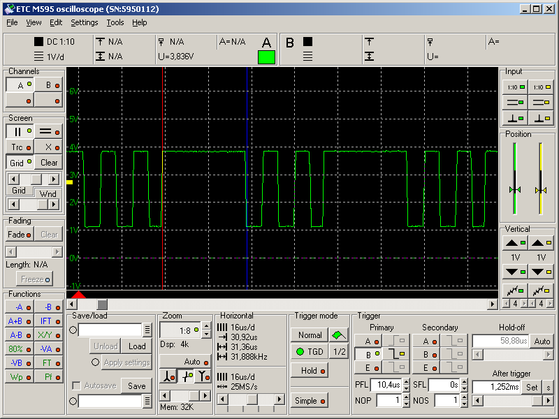
8.6 us turning time at the source ODW, 1.6 ms t.t. at the destination ODW
(green: input rectangle, yellow: output)
In this second example, the 8.6 us timeout at the source ODW (= timer started by a rising edge) does fire, and the positive-going pulse is cropped to 8.6 us in length - the rest is clamped to log.0 (as this happens at the source ODW, i.e. towards the dual-state optical bus). Note the glitch in the output, where the original edge was. Interesting. The 1.6 ms timeout at the destination ODW (= timer started by a falling edge) does not fire - the signal is faster than the timeout. Thus, the RS485 bus driver at the destination ODW doesn't ever turn off.
Now... what happens if you try to transport a permanent log.1 (hi level)?
AKA "break condition" in RS232 framing lingo. Does the output stay at log.1
forever? (Note that we're still speaking sync mode.)
You guessed it: no it doesn't. First the source ODW applies its turning time,
triggered by the one and only initial rising edge. When that times out,
the optical bus starts transmitting a log.0. The leading downward edge of
this log.0 gets evaluated by the destination ODW, and after another
instance of the turning time, the local RS485 transceiver lets go
(from log.0 to hi-Z).
...okay, so how do I set up the turning time, when I'm trying to use the sync mode for RS232 (async serial UART) framing? In case it doesn't want to work through the ODW's in normal async mode...
Sometimes it just so happens that you need to transport slightly non-standard RS232 framing, via Westermo ODW's, in sync mode (rather than the classic async mode with its nominal baud rate).
A good general rule of thumb with the ODW-700's (and probably ODW-600's as well) is to configure the turning time to be ten times the bit duration (or bit duration times the number of bits, that you'd normally configure in async mode). Not a single bit worth, but rather ten bits worth. This is because otherwise, an "all-zeroes" character (binary zero) could result in "turning too early".
Note that the resulting behavior is not identical to proper async mode
with a nominal baud rate.
In sync mode, the turning happens ten bit times after the last falling
edge - and that edge can be at different bit positions in the RS232 character.
In proper async mode, the turning occurs exactly 1 bit time after the
stop bit (after its trailing edge). It literally seems as if another
stop bit was added to the RS232 character (of course it does NOT disrupt
timing when characters are sent back-to-back, i.e. turning does not occur).
Take the following scope screenshot for example. The picture shows ASCII character "K" (our example throughout the following chapter) being transmitted at 19200 BPS, character format 8O1 (8 data bits, odd parity = 1 parity bit, 1 stop bit), through a pair of Westermo ODW's, configured for proper async mode, i.e. with baud and character format precisely specified. With Westermo, the character format is configured as "the number of bits to transfer" - parity is not closer specified nor inspected, to allow for "direct" transmission of parity-violating framings. So in our example, the "number of bits" is 11: because there's 1 start bit + 8 data bits + 1 parity bit + 1 stop bit. 1 bit time at 19200 equals 52 us.
ASCII character K at 19200, 8N1, ODW-600/ODW-700, proper async mode
(green: input, yellow: output)
Note that the output (after transmission) lags exactly 1 bit time
after the input (= 1 bit worth of transmission delay).
And, note that on the output side, the TX driver
turns off exactly 12 bit times after the start bit's leading edge.
I.e., the turning happens 1 bit time after the stop bit is over.
In the ASCII character 'K' above, the trailing pulse of log.1 in the
output waveform is exactly 3 bits wide: parity, stop bit, turning time.
Update from October 2012: Westermo have modified the "firmware" in the ODW-730 to transport the Break Condition correctly (just like the ODW-600 series). Thus, there is nowadays no difference anymore, between the ODW-700 and ODW-600 in how they handle the Break. The following text of this chapter is kept here for historical reference and for its general theoretical value.
In RS232 communications, there is a semi-illegal state called the Break condition. Break means that the transmitter (bus driver) holds the TX line in an "active" state (log.1 in Westermo polarity) for an indeterminate length of time (possibly many character times). This doesn't translate into any properly formed characters being transmitted - essentially it means that the physical layer is jammed in active state.
The Break condition is used by some fieldbus protocols or software suites to signal a bus reset, slave session end or some such - and it may be difficult to transport through data communications modems.
In async mode, there is a difference (no difference anymore,
see the update above!) in how the Break is handled by Westermo
ODW-700 series, compared to the older Westermo ODW-600 series. While the ODW-600
series do transport the Break just fine, the newer ODW-700 series do not -
the ODW-700 series clearly do not understand the Break condition,
and if presented with that, the output is a series of "false stop bits"
(or whatever it is).
See the waveforms below:
Break transported by ODW-600 in async mode (19200 bps)
(green: input, yellow: output)
Break transported by ODW-700 in async mode (19200 bps)
(green: input, yellow: output)
I should qualify this by "at the time of this writing". As the ODW logic is implemented in an FPGA (field programmable), it is possibly subject to later update.
You can also try transporting the Break using sync mode. In this case, you may want to set the turning time to the maximum possible value (1.6 ms) and see if that works for you = if a break this long is enough for your protocol to work. For instance, at 19200 bps, one bit time = 52 us, ten bits = 520 us, 1.6 ms is equivalent to about 3 characters.
If you're not exactly conversant in the RS232 basics, you may be wondering exactly what does the RS232 character framing look like, at the lowest level. Does the RS232 level converter flip polarity? What does it look like on RS422/485? That's a "balanced pair" transmission technology - does +/- matter, and is it standardized?
Let's have a recap :-)
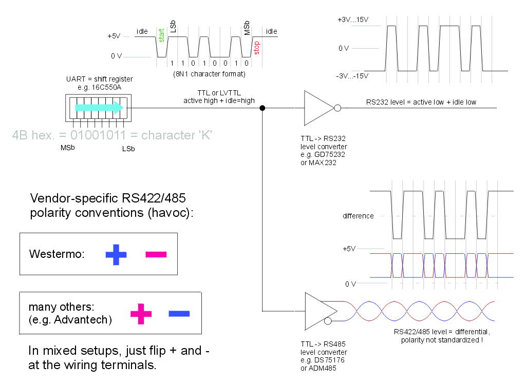
UART, RS232, RS422/485 framing and polarity - basics
Within our red-and-blue twisted pair line, Westermo puts the "+" label on the blue line, which is normally low, and shows a positive-going start bit (and payload). Note that this line typically corresponds to the inverting pin on the RS485 transceiver. Hence probably the polarity confusion (Westermo vs. the rest of the world). Note that Westermo's chosen "+" terminal follows the same polarity as RS232 single-ended signals.
At a first sight, or rather, upon a first focused consideration,
the character framing may look somewhat weird. But inevitably you have
to appreciate some beauty and ingenuity in its design. I myself am too
young to witness the era when this got introduced, so I don't have
that "age of innocence" and design decisions in my blood...
but I can see a few points:
Looking at the TTL level, i.e. UART output, the first striking thing
is the combination of "idle high level" (negative-going active traffic)
with "active high" encoding of data. Yeah right - polarity is arbitrary,
and the combination of data polarity vs. "framing overhead polarity"
also seems like a fairly random choice, doesn't make a difference...
Still it's interesting.
The start bit is "active" = has to "stick out" from the idle level.
That makes sense. The stop bit is "passive" = at idle level.
This is to make the stop bit different from the start bit, so that
there is always a clear signal edge on the boundary between two
consecutive characters, transmitted back to back (without a need for
some idle guard time or whatever). The combination of an active
start bit + passive stop bit also makes sure that regardless of the
combination of payload bits (data + parity), there is always at least
one active bit in the frame (= the start bit), at least some activity
going on, for the framing decoder (and possibly line drivers)
to sync on / work with.
Note that if you have significant EMI/noise on an otherwise idle
line, it will be evaluated as false start bits, as it is exactly
the start bit that "stands out from the idle background".
Both the TTL logic and RS232 line levels work with dual-state logic.
There's no third "OFF" state.
TTL is unipolar - it uses +5V for log.1 and 0V for log.0. The RS232 levels
are bi-poilar, "non return to zero" fashion. At RS232, zero volts is a forbidden
voltage level.
The RS232 line levels clearly assume a point-to-point full duplex interconnect
(there are no component-level logic gates on the market for those voltage levels)
but you cannot safely claim the same about the TTL logic. You can certainly
split a TTL-level RS232-framed signal to multiple destinations (gate inputs),
and, courtesy of the framing used, you can also combine this kind of signal
from several sources using AND gates (think of them as OR in inverted logic)
for a single input. This splitting/combining is often used in multi-format
industrial PC COM ports (232/422/485) - although actually the combination side
is often implemented using a jumper bank or mux, rather than an AND gate.
A typical RS232 transceiver chip
(D = line Driver, R = line Receiver with Schmitt trigger)
The RS422/485 is a "balanced pair" technology. The line drivers (and receivers)
are nowadays implemented using special-purpose transceiver IC's, such as the
venerable DS75176, ADM485 or compatibles. The wires in the pair do not
"flap about" the reference ground - rather, each wire switches between
two positive voltage levels: one is close to ground (0V), the other is close
to +5V. The decision treshold is +/- 200 mV differential with schmitt trigger.
The drivers are powered by +5V against GND and use a "full totem pole"
on each output, which can be turned into a "high-impedance" third state
by an auxiliary input pin (TX_enable) which turns both transistors
in the totem off at the same time.
The receiver side can typically work in a differential fashion between
about -3 and +7 Volts -- i.e., differential signals do not get
"clipped" as soon as they wander out of the box defined by the transceiver's
0V and +5Vcc.
A typical RS485 transceiver chip
Looking at the previous sketch of RS485 polarity/wiring, you may have
a follow-up question/complaint:
"So... where does the turning take place? It's the most prominent buzzword in this paper,
and it doesn't show up in your sketch?"
We're getting to that point right now. Let's have another sketch - in the scope trace illustration you can see the 485 transceiver turning on and off, and you can see more explanatory schematic goodies around.
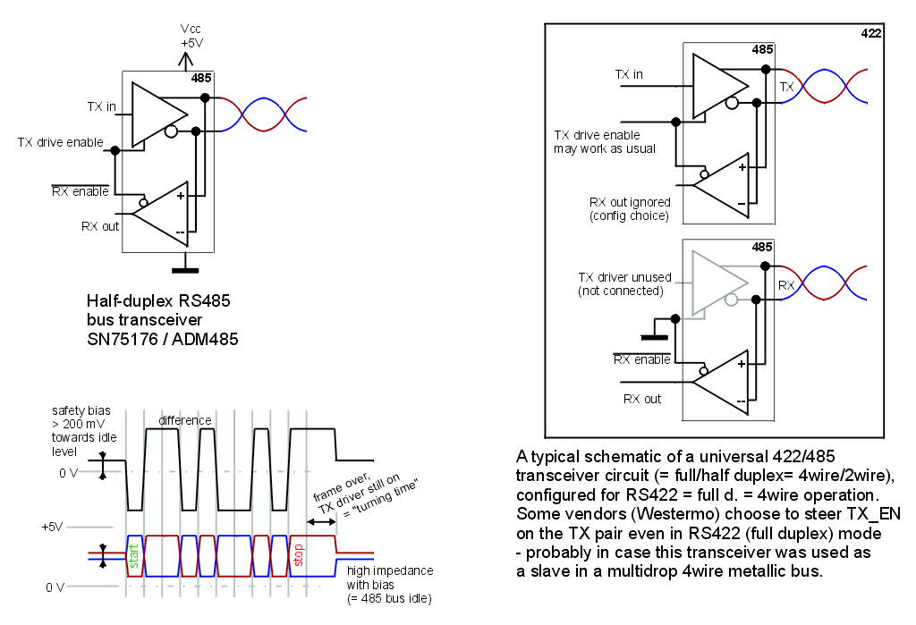
RS485 RX/TX steering, AKA "turning" in Westermo lingo
The TX_en / ~RX_en signals can be driven by the PC UART's TEMT pin (see OX16C950 or LPC SuperIO by Fintek or SMSC), or by some single-shot circuit (re)triggered by the TX signal, or by some custom logic that knows the baud rate and understands the framing (an FPGA inside a Westermo converter box). Or, after all, by software.
Note how the full-duplex RS422 transceiver circuit (actually universal 422/485)
is combined out of two RS485 integrated circuits, where the TX part of the
transceiver IC used for "RS422 RX" is inactive/unused/ignored.
Note that even in RS422/4-wire mode, the TX pair tends to turn its driver
on and off - probably to allow the transceiver to work as a "slave node"
in a 4wire metallic bus.
Okay - so we have turning in the picture. Now... why doesn't the line
return to 0V differential when idle / in high impedance?
Why are the blue and red traces apart when idle?
Is that to make them more distinct in the sketch?
No it's not a drawing imperfection. It's called a "bias".
There is indeed a non-zero voltage on the RS485 line when idle - and it's there for a reason. At least - it should be on the line, to make it more reliable. It's called a "bias", and is implemented by a resistive divider, stretching the line a bit towards +5V and reference ground. It's two more resistors, on top of the notorious 120Ohm terminators. The power supply for biasing can be external, and unlike the terminators, the biasing resistors can be placed anywhere on the bus - yet typically the bias power is taken from one of the transceivers involved (= this is where the biasing totem is collocated).
Westermo have a special buzzword for the RS422/485 line bias: they call it "fail-safe". And in the manuals of their ODW-600/700 series, it is misdocumented (at the time of this writing). The following sketch shows a nearly complete schematic of the Westermo ODW RS422 bus transceiver, with the S3 jumpers vs. RS422 wiring terminals precisely matching reality (investigated using an Ohm-meter):
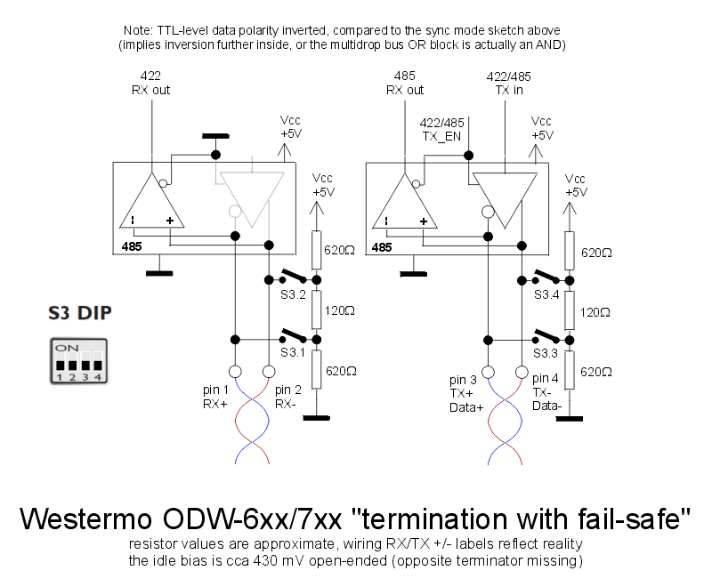
Westermo "Termination with fail-safe" - addendum to the user's guide
The sketch implies, that to properly terminate a 4wire line on a Westermo ODW, you need to turn on all the four switches in the DIP bank labeled S3.
The sketch further implies, that the blue line in the signal pair (labeled "+" by Westermo) is actually biased slightly negative when idle - with a positive-going start bit and payload.
Speaking of wiring terminals, note that the ODW-600/700 series lack a reference ground terminal on the RS422/485 metallic port. If you ever get into trouble and are wondering if perhaps the missing ref.gnd is the culprit, there is a way to get your hands on the ODW transceiver's ref.gnd, at least for the purpose of an improvised test, if not for routine operation.
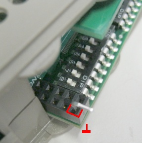
Westermo ODW-600/700 series RS485 reference ground
This is made possible by the fact that the ODW's small-signal internals (FPGA etc) share a PSU+ground domain with the local RS422/485 port. There's an isolation gap that isolates this PCB island from the PSU primary, and the fiber optical ports are isolated inherently (need no isolation). The tap in the photo uses pin 2 in the ODW's debug connector.
May this trick serve you well. It's quite likely that in a practical troubleshooting scenario, it will help you to make sure that the missing ref.ground is not a problem this time - certainly provided that your RS422 port provides bias (fail-safe) to the bus. Ahem - which may not necessarily be true, as the bias is legcuffed to the terminator...
The "fail-safe"(TM) feature (=bias), inherently linked to termination
in the Westermo ODW converter boxes, keeps the line conveniently
in the "inactive" logical level, just outside of the forbidden zone of the
receiver's Schmitt trigger - all of that in the high-Z state on the bus.
Polarity of the bias seems compatible, despite the nominal +/- misunderstanding
with the rest of the world. I.e., once you get the +/- wiring functional
with your other RS485 devices, the bias should also be compatible,
even if there's another device also providing bias.
Apart from its generic purpose = keeping the line clean of random EMI,
fail-safe/bias helps the "OR-style combination logic" on the optical bus
and the "turning" at the destination ODW to work correctly.
The way "turning" works in sync mode has an interesting "side effect":
no single node on the "optical bus" can jam the bus by accidentally
getting stuck active at a single voltage level (log.0 or log.1).
If stuck at log.1, it gets quickly gated by the turning time.
If stuck at log.0, that's a non-issue.
Compared to that, note that in async mode, a node transmitting
a "break" will disrupt the bus (regardless of ODW-600/700 series).
With the local metallic ports on the ODW's configured for 4wire operation, and with the slave nodes configured for "V mode", the "turning" mechanism does not in any way prevent/preclude full duplex operation between the master node and any slave node. Turning may happen, but will not disrupt the original flow of logical ones and zeroes, because
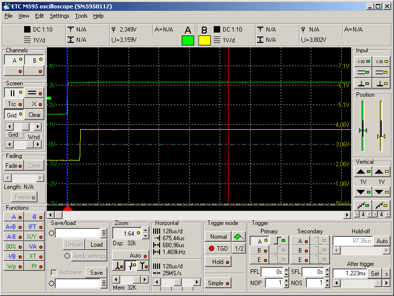
The following scope screenshot shows our original test signals (rectangles), that have passed through our V-mode test rig in opposite directions, simultaneously. This is to prove that full duplex indeed works as advertised.
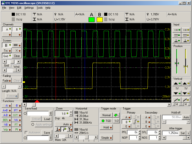
Westermo ODW-730 running full duplex in sync mode, t.t.=1.6ms
(green: output in direction A, yellow: output in direction B)
Published: September 17th 2012